- 您现在的位置:买卖IC网 > Sheet目录1996 > HSP45102SC-40Z (Intersil)IC OSC NCO 40MHZ 28-SOIC
6
FN2810.9
April 25, 2007
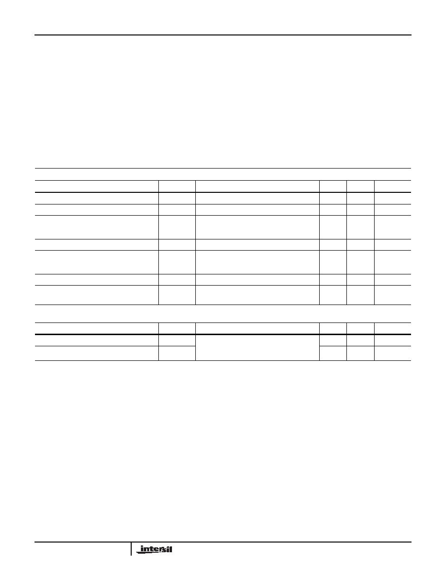
Absolute Maximum Ratings TA = +25°C
Thermal Information
Supply Voltage. . . . . . . . . . . . . . . . . . . . . . . . . . . . . . . . . . . . . +6.0V
Input, Output or I/O Voltage Applied . . . . .GND -0.5V to VCC +0.5V
ESD Classification . . . . . . . . . . . . . . . . . . . . . . . . . . . . . . . . . Class 1
Operating Conditions
Operating Voltage Range (Commercial, Industrial). . +4.75V to +5.25V
Operating Temperature Range (Commercial) . . . . . . . 0°C to +70°C
Operating Temperature Range (Industrial) . . . . . . . .-40°C to +85°C
Thermal Resistance (Typical, Note 1)
θJA (°C/W)
SOIC Package . . . . . . . . . . . . . . . . . . . . . . . . . . .
70
Maximum Junction Temperature . . . . . . . . . . . . . . . . . . . . . . +150°C
Maximum Storage Temperature Range . . . . . . . . . . -65°C to +150°C
Pb-free reflow profile . . . . . . . . . . . . . . . . . . . . . . . . . .see link below
Die Characteristics
Backside Potential . . . . . . . . . . . . . . . . . . . . . . . . . . . . . . . . . . . VCC
CAUTION: Stresses above those listed in “Absolute Maximum Ratings” may cause permanent damage to the device. This is a stress only rating and operation of the
device at these or any other conditions above those indicated in the operational sections of this specification is not implied.
NOTE:
1.
θ
JA is measured with the component mounted on an evaluation PC board in free air.
DC Electrical Specifications
PARAMETER
SYMBOL
TEST CONDITIONS
MIN
MAX
UNITS
Logical One Input Voltage
VIH
VCC = 5.25V
2.0
-
V
Logical Zero Input Voltage
VIL
VCC = 4.75V
-
0.8
V
High Level Clock Input
VIHC
VCC = 5.25V
3.0
-
V
Low Level Clock Input
VILC
VCC = 4.75V
-
0.8
V
Output HIGH Voltage
VOH
IOH = -400μA, VCC = 4.75V
2.6
-
V
Output LOW Voltage
VOL
IOL = +2.0mA, VCC = 4.75V
-
0.4
V
Input Leakage Current
II
VIN = VCC or GND, VCC = 5.25V
-10
10
μA
Standby Power Supply Current
ICCSB
-
500
μA
Operating Power Supply Current
ICCOP
f = 33MHz, VIN = VCC or GND
-99
mA
PARAMETER
SYMBOL
TEST CONDITIONS
MIN
MAX
UNITS
Input Capacitance
CIN
FREQ = 1MHz, VCC = Open. All
measurements are referenced to device
ground
-10
pF
Output Capacitance
CO
-10
pF
NOTES:
2. Power supply current is proportional to operating frequency. Typical rating for ICCOP is 3mA/MHz.
3. Not tested, but characterized at initial design and at major process/design changes.
4. Output load per test load circuit with switch open and CL = 40pF.
HSP45102
发布紧急采购,3分钟左右您将得到回复。
相关PDF资料
HSP45106JC-33Z
IC OSC NCO 33MHZ 84-PLCC
HSP45116AVC-52Z
IC OSC NCO 52MHZ 160-MQFP
ICL7109EPL+
IC ADC 12BIT 3-ST 40-DIP
ICM7217AIPI
IC OSC UP/DWN CNTR 2MHZ 28-DIP
ICM7217CIPI
IC OSC UP/DWN CNTR 2MHZ 28-DIP
ICM7242IPA
IC OSC BINARY CTC 13MHZ 8-DIP
ICM7250IWE+T
IC OSC BINARY CTC 15MHZ 16SOIC
ICM7556IPD
IC OSC TIMER DUAL 500KHZ 14-DIP
相关代理商/技术参数
HSP45102SI-33
制造商:Rochester Electronics LLC 功能描述:12 BIT NUMERICALLY CONTROLLED OSCILLATOR - Bulk
HSP45102SI-3396
功能描述:可编程振荡器 12 BIT NCO 28LD SOIC,T&R,33MHZ,IND RoHS:否 制造商:IDT 封装 / 箱体:5 mm x 7 mm x 1.5 mm 频率:15.476 MHz to 866.67, 975 MHz to 1300 MHz 频率稳定性:+/- 50 PPM 电源电压:3.63 V 负载电容:10 pF 端接类型:SMD/SMT 输出格式:LVPECL 最小工作温度:- 40 C 最大工作温度:+ 85 C 尺寸:7 mm W x 5 mm L x 1.5 mm H 封装:
HSP45102SI-33Z
功能描述:可编程振荡器 W/ANNEAL 12 BIT NCO 28 33MHZ IND RoHS:否 制造商:IDT 封装 / 箱体:5 mm x 7 mm x 1.5 mm 频率:15.476 MHz to 866.67, 975 MHz to 1300 MHz 频率稳定性:+/- 50 PPM 电源电压:3.63 V 负载电容:10 pF 端接类型:SMD/SMT 输出格式:LVPECL 最小工作温度:- 40 C 最大工作温度:+ 85 C 尺寸:7 mm W x 5 mm L x 1.5 mm H 封装:
HSP45102SI-40
制造商:Rochester Electronics LLC 功能描述:- Bulk
HSP45106
制造商:INTERSIL 制造商全称:Intersil Corporation 功能描述:16-Bit Numerically Controlled Oscillator
HSP45106/883
制造商:INTERSIL 制造商全称:Intersil Corporation 功能描述:16-Bit Numerically Controlled Oscillator
HSP45106_04
制造商:INTERSIL 制造商全称:Intersil Corporation 功能描述:16-Bit Numerically Controlled Oscillator
HSP45106883
制造商:INTERSIL 制造商全称:Intersil Corporation 功能描述:16-Bit Numerically Controlled Oscillator